See Every Detail, At High Speed
Because in the semiconductor industry, “almost perfect” is simply not good enough.
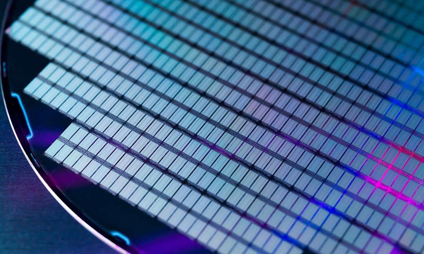
Precision is everything in wafer manufacturing. As wafer structures become smaller and smaller and production lines run faster and faster, other imaging systems often reach their limits. Detecting macro defects (> 1 µm) on large wafers at high speed and with the right lighting has become one of the biggest challenges in quality assurance.
Discover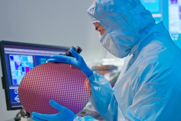
Application Examples: Flexible Inspection - Across All Wafer Process Steps
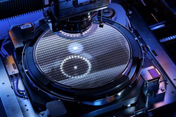
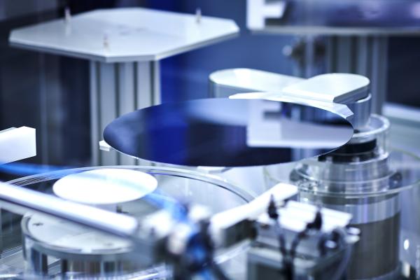
From bare wafers to final delivery, visual inspection is essential at every stage. These are typical areas of application where high-resolution imaging and customized lighting make all the difference.
Bare Wafer Inspection
Inspection of unprocessed wafers for particles, surface scratches, or contaminants before structuring begins.
Backside Wafer Inspection
Quality control of the wafer reverse side – important before processing or for double-sided wafers.
Macro Defect Detection
Detection of large-area defects such as coating irregularities, poor contacts, bridging, or missing structures.
Etch Process Monitoring
Inspection after the etching step to detect residues, corrosion, pinholes, or pattern defects.
CMP (Chemical Mechanical Polishing) Inspection
Surface quality control after polishing - checking for scratches, residues, or unpolished areas.
Outgoing Quality Control
Final visual check before wafers leave the fab - ensures cleanliness, coating integrity, and surface quality.
Contact Our Experts Now!