See through silicon.
Reveal the unseen, catch defects sooner.
Visible light leaves blind spots in semiconductor inspection. Short wave infrared closes them - exposing subsurface defects, material differences, and alignment features across your line. Our end-to-end SWIR portfolio integrates from lab to in line AOI, helping you catch issues earlier, protect yield, and ship with confidence.
Discover our SWIR camera portfolioApplication Examples in Semiconductor Production and Inspection
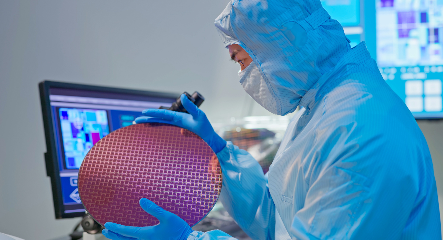
From bare wafers to final delivery, visual inspection is essential at every stage. These are typical areas of application where high-resolution imaging and customized lighting make all the difference.
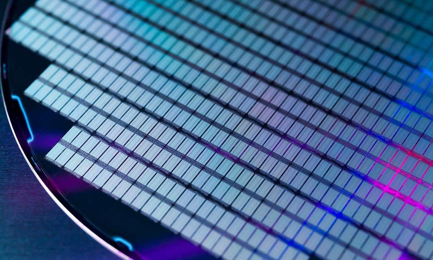
Bare and patterned Wafer Manufacturing
- Detection of microcracks and subsurface damage in wafers
- Through-wafer imaging of internal and front-side structures (e.g., for alignment)
Advanced Packaging
- Detection of hidden defects in bonded or stacked structures
- Inspection of die attach quality and underfill voids
Wafer or Die Bonding
- Precise alignment of marks through silicon for wafer to wafer and die to wafer bonding.
- Detection of voids, particles, bubbles, and delamination after bonding.
Diced Die Sorting and Inspection
- Identification of microcracks from sawing or laser dicing, including subsurface and edge damage
- Die quality grading prior to packaging


Why SWIR?
See more. Achieve more.
Infrared radiation lies between visible light and microwaves on the electromagnetic spectrum, with short-wave infrared (SWIR) covering wavelengths from 0.9 to 2.5 μm. Although SWIR radiation is not visible to the human eye, it interacts with objects like visible light, enabling cameras to "see" through various materials and in challenging environments.
Indium Gallium Arsenide (InGaAs) based sensors are very popular to detect light in the SWIR range. They enable you to:
- see through silicon and many packaging materials at SWIR wavelengths
- differentiate coatings, adhesives, and contamination that look identical in visible light
- see in low-light, dust, or haze
- provide high image quality enhanced by our uniformity correction, low noise, and the right cooling for longer exposures.
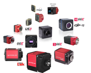
Our SWIR Camera Portfolio
Allied Vision provides one of the most-comprehensive SWIR camera portfolios on the market supporting area- and line-scan SWIR sensors. Select from single boardlevel options to housed models with compact form factor and up to scientific grade solutions with strong sensor cooling and sensitivity up to 2.2µm.
Click on the camera series and find out more!
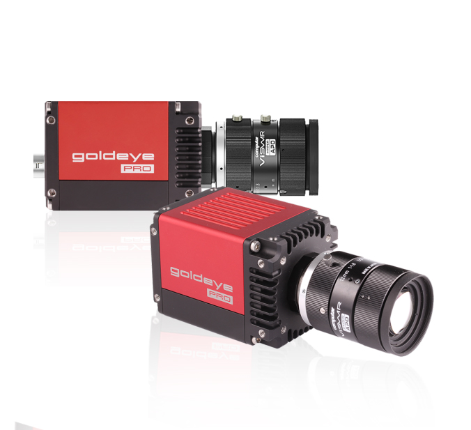
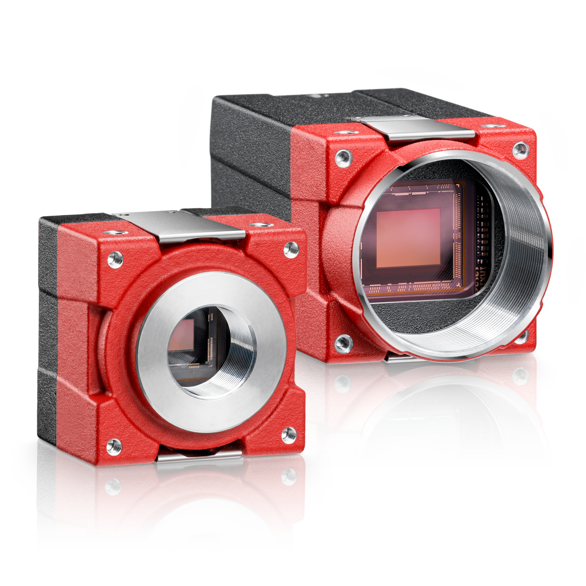
Goldeye/Goldeye Pro - Excelence in SWIR Imaging
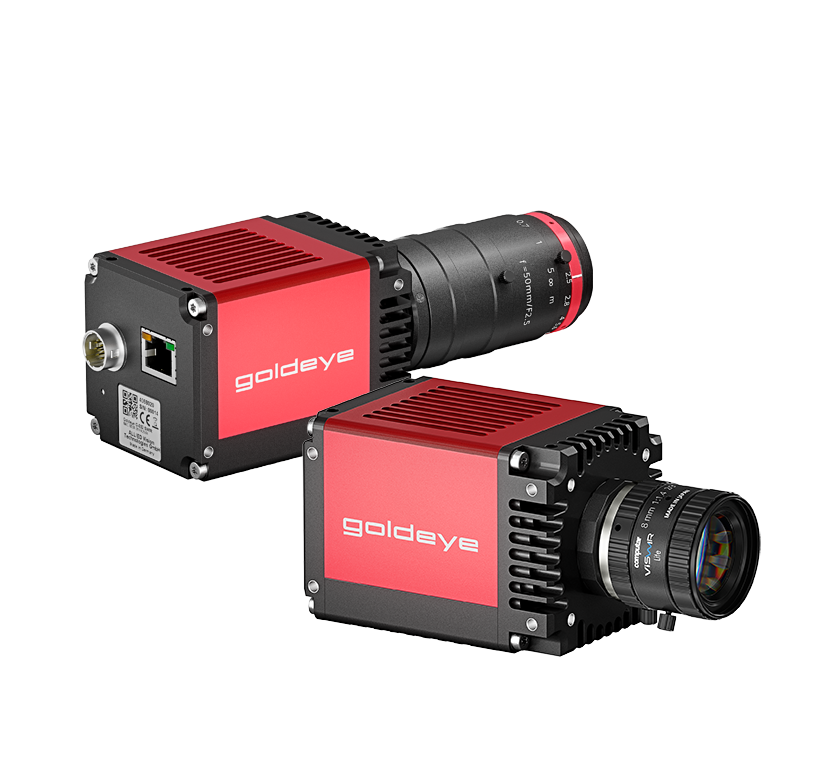
Goldeye - Versatile High-performance SWIR Platfrom
- Two housing designs: compact industrial (55mm x 55mm x 78mm) and advanced scientific (90 mm x 90 mm x 80 mm) for demanding applications
- Support of numerous InGaAs sensors with TEC1 or TEC2 cooling including IMX990/991 Sony SenSWIR sensors
- Models with strong sensor cooling down to -30°C for long exposure times or eXtended SWIR sensitivity up to 2,200nm
- Standard compliant GigE Vision and Camera Link interfaces
- Advanced image correction features including Non-Uniformity, Defect Pixel, and Background Correction. NUC and DPC sets are applied instantaneously (from image to image).
Outstanding image quality with high dynamic range (up to >70dB)
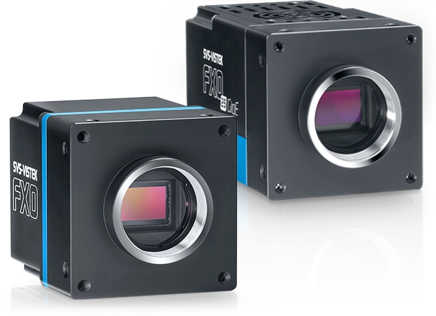
FXO - SWIR Imaging with Highest Throughput
Alvium - Compact, Flexible, and Affordable SWIR
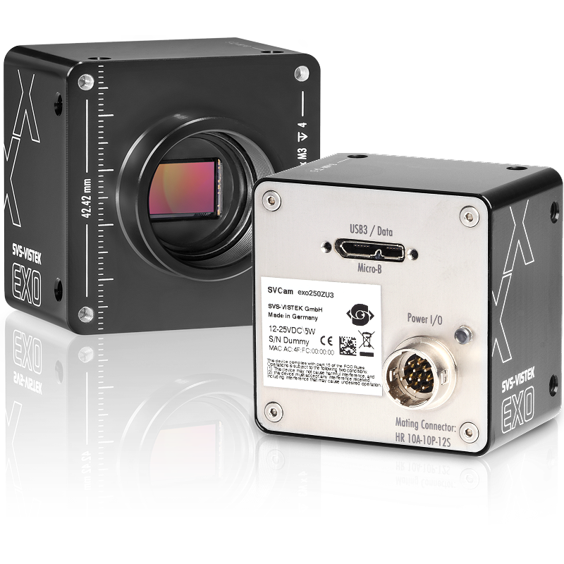
exo - Accessible Industrial SWIR Imaging
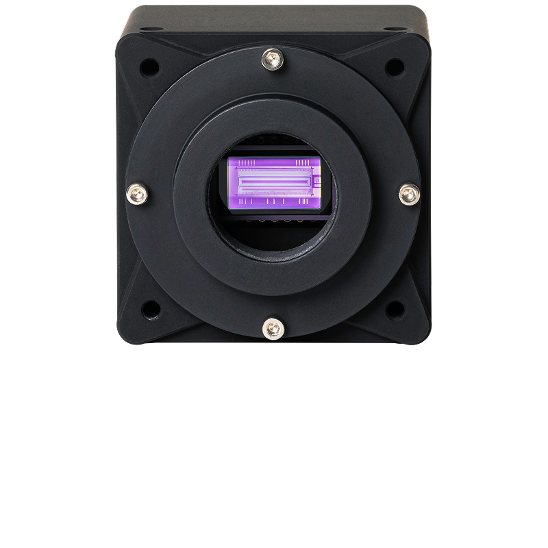
allPIXA SWIR - GigE-based Line-scan SWIR Imaging

Machine Vision Software libraries for typical applications
eVision is a set of hardware-independent image processing and analysis libraries for machine vision inspection applications. Our Machine Vision Software is compatible with any image source, including frame grabbers, GigE Vision, and USB3 Vision cameras. The general-purpose libraries cover SWIR applications such as:
Matching and Measurement
- EasyFind: Geometric pattern matching
- EasyGauge: Sub-pixel measurement & dimension control
- EasyMatch: Pattern matching using normalized correlation
- EasySpotDetector: Detection of faint defects and contamination
Deep Learning Libraries
- EasySegment: Defect detection and segmentation
- EasyLocate: Localization and identification of objects, products, or defects in the image
- EasyClassify: Classify images after learning/training process

Get Support
Whether you are looking for a single component or a complete solution for your SWIR imaging inspection application in the semiconductor industry, our team will support you in finding the right solution for you.
