
Advanced Wafer Inspection for High-Resolution, High-Speed Defect Detection
Trends such as the miniaturization of products and higher production speeds lead to increasingly complex challenges for manufacturers of semiconductor components. They must keep a close eye on the cost-efficiency of their processes to remain competitive.
Read Whitepaper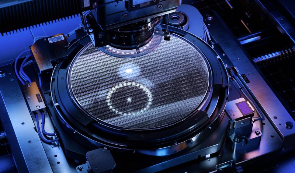
Learn How To Maximize Throughput And Minimize Defects
Anyone aiming to manufacture wafers cost-effectively must ensure high yield in production. It is therefore essential to detect yield-reducing defects as early as possible in order to adapt further processing and avoid unnecessary costs from performing production steps on already defective components.
This White Paper aims to highlight the technical possibilities of machine vision in the semiconductor industry and present solutions for this specific area of application.
You will learn more about:
- Key challenges in high-throughput wafer inspection environments
- Detection of macro defects impacting yield and process stability
- High-resolution line scan imaging for scalable inspection of 300 mm wafers
-
Let's Talk About Your Application