Applications
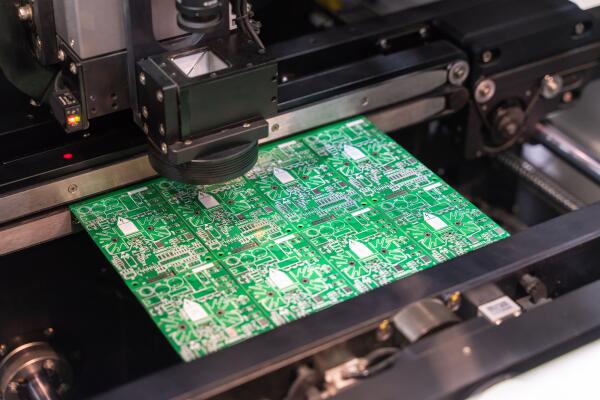
Electronics, FPD & Semiconductors
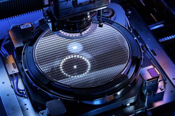
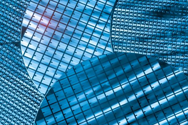
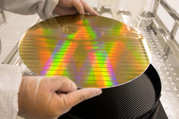
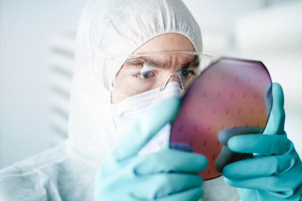
Semiconductor Inspection
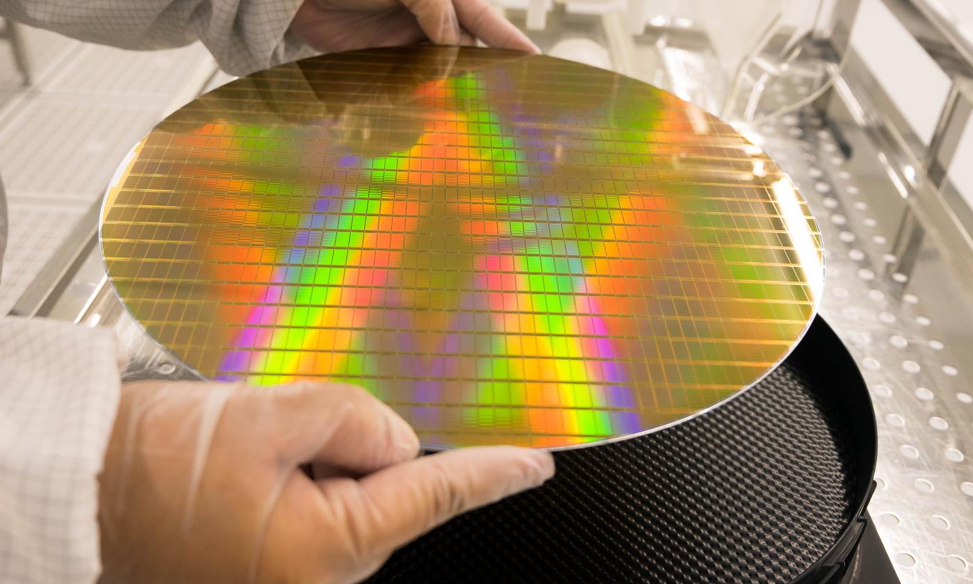
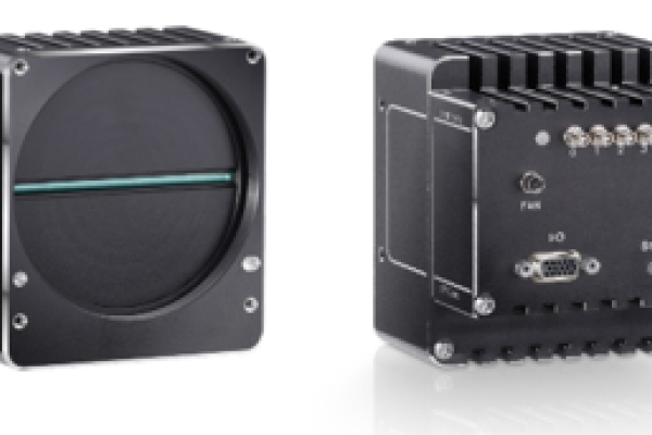
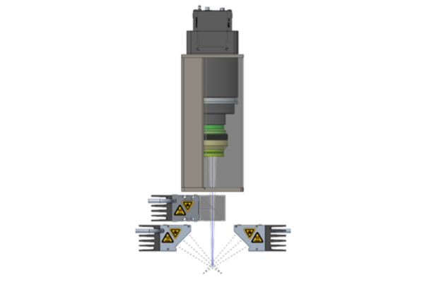
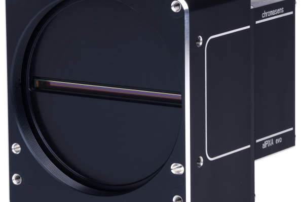
Semiconductor Inspection Cameras For Advanced Wafer Surface Analysis
Detect Defects Precisely For Consistent, High-Quality Semiconductor Output
Achieve superior semiconductor quality with industrial cameras designed for precise inspection. Enhance defect detection and process reliability in production.
Technical Requirements
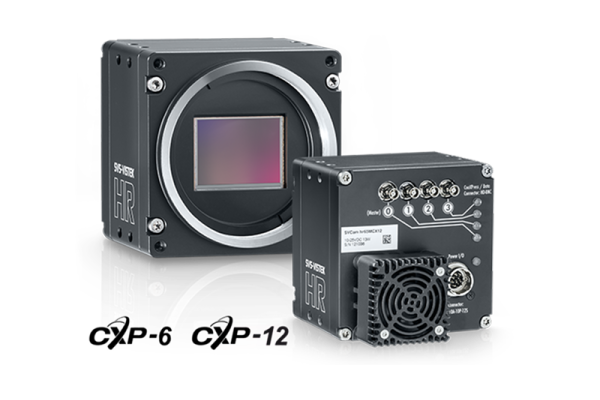
- High spatial resolution imaging for reliable defect detection in wafer or semiconductor production
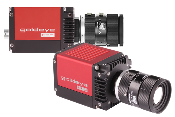
- SWIR sentitive cameras seeing through all layers with the highest levels of accuracy
- High bandwidth for semiconductor inspection requiring high-definition imaging
- State-of-the art sensors running at high frame rates for increasing production throughput

Do you have any questions? We are here to help.